Understanding Mobile Motherboards
10 April 2025
CH Imtiaz Ahmed
8 MIN READ
SHARE PROTOCOL
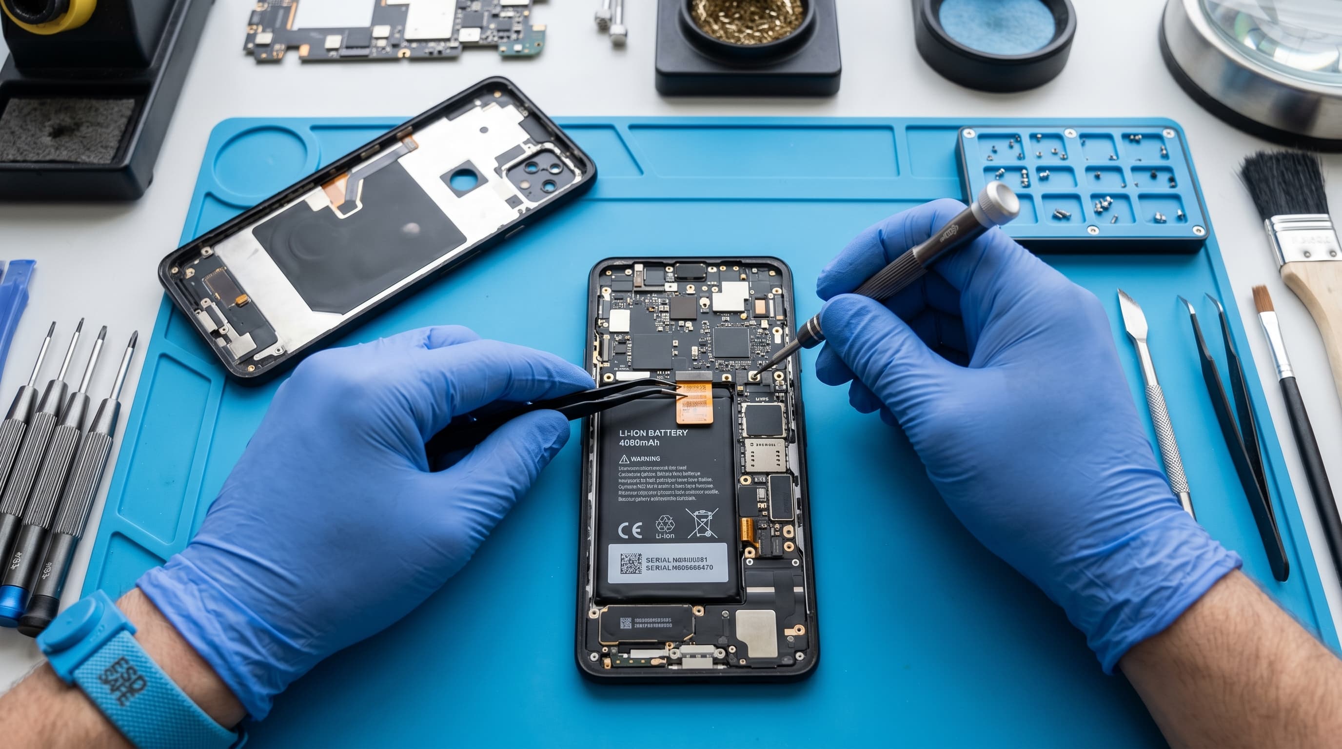
A modern smartphone motherboard is a marvel of dense multi-layered engineering, containing over 10 layers of microscopic copper traces squeezed into an incredibly small footprint.
Core Architectural Blocks The brain of the board is the SoC (System on Chip) or Application Processor (AP), which is often stacked in a "double-decker" configuration directly underneath the RAM chip to reduce communication delay. Surrounding it are dozens of smaller, highly critical integrated circuits.
Power Management (PMIC) The PMIC (Power Management Integrated Circuit) takes the raw battery voltage (usually 3.8V - 4.2V) and steps it down through complex buck converters and LDO regulators to produce lower voltages (e.g., 1.8V, 1.1V, 0.8V) required by the processor and other subsystems.
Signal & RF Subsystems Other major blocks include the Baseband Modem (handling network signal synthesis), the RF Transceiver (radio frequency filtration), and the Audio Codec. Understanding these blocks allows you to isolate faults systematically instead of heating random components with a hot air gun.
Topical Reference Tags
#motherboard#soc#pmic#architecture#diagnostics